How modular architectures are redistributing power in semiconductors
Semiconductors are entering a structural shift. As monolithic scaling slows, heterogeneous integration and advanced packaging are redefining where systems are built and where value is captured.
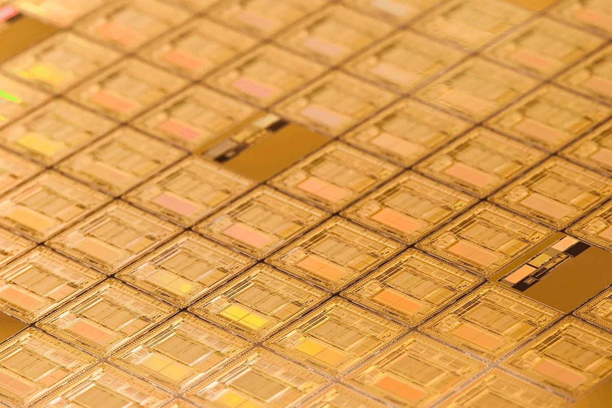
The integration boundary is moving up the stack and no longer sits at the die. Instead, it is shifting toward the multi-die package in leading segments at the full accelerator module.
There is clear evidence that advanced packaging is growing revenue materially faster than front-end wafers. In AI, the fully integrated accelerator module captures multiples of the standalone compute die. During recent demand surges, advanced packaging capacity has constrained revenue, not wafer supply. In concentrated markets, control of the system boundary compounds pricing power.
Architecture drives industry structure, which determines profit pools. The companies that control the integration boundary will control the next decade of semiconductor economics.
Leaders must respond deliberately by defining their role in the modular stack and moving integration decisions upstream into architecture governance. Leaders can also invest in bottlenecks like advanced packaging and substrates, while building consistent lifecycle discipline across chiplet and module families.
Integration is no longer a manufacturing detail, but a strategic control point that defines commercial value.
Defining the integration boundary
The integration boundary is the point in the stack where architectural control, commercial accountability, and system validation converge.
It can sit at several levels:
Discrete die
Multi-die package
Board-level module
Full platform
For decades, the die defined the product while performance and density drove advantage.
In modular architectures, the product is a validated system-in-package assembled from specialized dies across nodes and suppliers. The economic center of gravity moves with that shift.
Architecture is moving up the stack
Monolithic scaling delivered predictable cost and performance improvements. That model is now under pressure.
Larger dies increase yield risk as capital intensity escalates and functions scale at different rates; memory, logic, and analog do not share the same economics.
The unit of optimization is no longer the transistor, but the system.
This system is visible in capital flows. Advanced packaging revenues are expanding at roughly double the growth rate of front-end wafer revenues in leading-edge segments. Investment is shifting toward integration technologies: 2.5D, 3D stacking, high-density substrates, and chiplet interconnect standards.
That architectural locus of control is rising.
Integration multiplies economic power
The shift is most visible in AI infrastructure, where workload demands are redefining semiconductor value.
AI training and inference require extreme memory bandwidth, low-latency interconnects, and sustained thermal performance, pushing value beyond the standalone GPU die. While GPU dies often sell for a few thousand dollars, a fully integrated AI accelerator module can sell for orders of magnitude higher since it combines compute, HBM, advanced packaging, and system-level validation. The incremental value is not in additional transistors alone, but in system-level integration:
Memory stacking and bandwidth
Die-to-die interconnect performance
Thermal density management
Full-system validation and software alignment
Customers do not buy discrete silicon; they buy validated subsystems.
Integration changes the economics in four ways:
Reduces substitutability: a validated module is harder to replace than a die.
Increases switching costs: qualifications shift from component level to system level.
Concentrates system accountability: warranty and performance liability move upward.
Expands share of wallet: the integrator captures a larger share of the system BOM.
Constraint points define structural leverage
The recent AI surge exposed multiple bottlenecks across the semiconductor value chain, from HBM memory supply to data center capacity. Some of these constraints are beginning to ease, but advanced packaging will constrain delivery of full accelerator modules that unlock the next step in GPU die value.
Lead times for advanced packaging expanded sharply during peak demand periods, even when wafer capacity was available. When integration capacity constrains shipments, it also stalls value realization across the entire chain.
As a result, the bottleneck layer becomes the control layer.
Control of constrained integration capacity determines:
Allocation across customers
Priority access to roadmap nodes.
Negotiation leverage in pricing discussions.
Which platforms scale and which stall.
In performance-driven markets, control of the constraint point defines structural power.
The automotive precedent
Automotive offers a useful structural analogue. As vehicles became more electronically complex, automakers moved from managing large numbers of discrete components toward integrated module subsystems to reduce coordination costs, improve reliability, and simplify accountability. In that shift, value did not merely consolidate; it migrated toward the Tier-1 integrators who controlled the modules, defined the interfaces, and assumed warranty responsibility.
The sequence was consistent:
Architectures modularized.
Interfaces formalized.
Accountability shifted upward.
Profit pools consolidated at integration layers.
Semiconductors are entering a similar phase in AI, automotive computing, high-performance computing, and industrial infrastructure. As companies continue modularizing architecture, integrators accumulate more leverage.
Where new control points are solidifying
As the package becomes the system boundary, new profit pools concentrate at identifiable control points.
Architectural control: ownership of die partitioning, chiplet interfaces, and socket definitions shapes ecosystem participation and long-term compatibility.
System validation: advanced packaging capacity, substrate supply, and high-density interconnect technologies are gating enablers. Constrained layers dictate allocation and scale.
Commercial accountability: lifecycle management, validation frameworks, and revision governance create switching costs in end-markets (e.g., automotive, infrastructure, etc.).
Each reinforces the same structural outcome: economic power concentrates where integration, accountability, and constraint intersect.
Strategic imperatives for semiconductor leaders
This shift is structural and requires a structural response.
Commit to a role: choose whether to be a platform owner, module integrator, specialist supplier, or constrained-technology enabler. Avoiding the decision defaults you to a replaceable component role with limited pricing power.
Move integration upstream: embed packaging, partitioning, and interface governance into early architecture decisions. Integration cannot remain a downstream manufacturing consideration.
Invest at constraint points: identify the bottleneck layers in your segment, packaging capacity, substrates, interconnect IP, and validation structure. Your negotiation will be limited if you aren’t proactive about the constraint.
Institutionalize lifecycle discipline: treat chiplets and modules as managed product families. Develop compatibility standards and roadmap governance deliberately to build durable switching costs.
Build integration capability: standardize cross-functional integration across design, packaging, manufacturing, and validation. Integration must be a repeatable operating capability, not an ad hoc project.
Closing perspective
The semiconductor industry is not only advancing but also undergoing structural reorganization.
Advanced packaging is outpacing front-end growth in critical segments. System-level platforms command multiples of discrete die value. Integration capacity has become a binding constraint. Market concentration amplifies control at the system boundary.
In monolithic eras, transistor leadership defined advantage. In modular eras, integration control defines it. The integration boundary is where architectural authority shapes structure, structure shapes leverage, and leverage shapes profit.
The companies that own the integration boundary will own the economics of the next decade.
Contributing author: Emery Engling
With two decades of semiconductor experience, Simon-Kucher has supported industry leaders through transformative cycles, from the rise of the data economy to AI acceleration, and to the global compute surge. We are well-positioned to anticipate what comes next and excited to serve as a strategic partner in shaping it.